


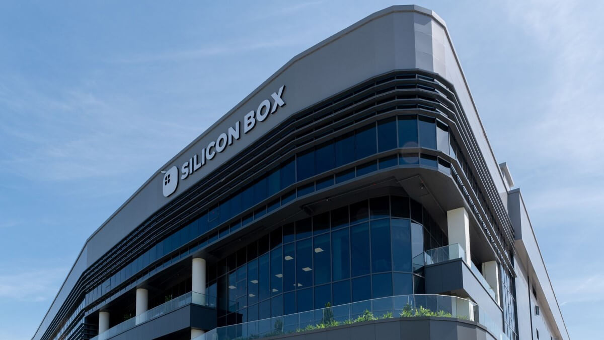
The Singapore-based semiconductor manufacturer Silicon Box has announced intentions to invest 3.2 billion euros (approx. $3.6 billion) in building a manufacturing plant in northern Italy, a historic step that would strengthen Italy’s standing in the global tech scene. This government-backed investment represents a major milestone in Italy’s ongoing campaign to lure high-tech investments to its shores.
Although the precise location of the new facility in the country’s north is still up in the air, a number of possible locations are now under consideration. The facility’s design and planning will start right now, and building will start if the European Commission approves the Italian State’s proposed financial contribution.
Nearly three years into the semiconductor business, Silicon Box was created by former employees of the massive American chip manufacturer Marvell. The company is focused on creating ‘chiplets’ – small semiconductor fragments around the size of a sand grain. These chiplets are put together using cutting-edge packaging methods, which are an innovative and economical way to build processors with a lot of power. These processors can power a vast range of use cases, from complex data centers to common domestic appliances.
This ambitious initiative would not only demonstrate Silicon Box‘s pioneering position in the future of semiconductor technology but also Italy’s increasing attractiveness as a location for tech investment. In addition to the approximately 1,600 semiconductor jobs at Silicon Box’s new manufacturing facility, the project is expected to create thousands of jobs for contract construction companies and indirect suppliers.
AI, Edge Computing, LLM
“We believe innovation is driven by cultural values that embrace curiosity, passion, and a tireless commitment to excellence,” said Dr. Byung Joon (BJ) Han, co-founder and CEO of Silicon Box. “Italy was one of our top choices for global expansion because we found that its culture shares our values. We have seen great promise through our collaborations with the Italian government and various regional, institutional, and commercial stakeholders to date, which we know will be necessary to successfully execute this first-of-a-kind project in Europe.”
“We are excited to bring Italy to the forefront of chiplet deployment and the semiconductor industry, through this investment into the world’s most advanced packaging solution,” said Dr. Sehat Sutardja, co-founder and Chairman of Silicon Box. “It will enhance competitive strengths in design, artificial intelligence (AI), large language models (LLMs), electronic vehicles (EVs) and automotive, mobile, wearables, smart consumer, edge computing, and material sciences of the Italian ecosystem, and revolutionize Europe’s position in the global [semiconductors] supply chain. Throughout my career, I have always been a big believer in Italian and European ingenuity.”
Advanced Packaging
“Italy was chosen as the location for Silicon Box’s first global expansion for several reasons, including its infrastructure, strong talent base and the government’s initiative to support and streamline the business environment and key stakeholder conversations,” added Dr. Han. “The competitive jobs that Silicon Box’s new facility will create will include engineers, equipment technicians, factory operators, and business functions. Italy offers an exceptional ecosystem for higher education with strong traditions in various engineering disciplines. This was a decisive factor in Silicon Box’s choice to build in Northern Italy and will be essential to our long-term success.”
Wafer fabrication facilities, often known as ‘fabs,’ use a variety of sophisticated techniques to build semiconductors on silicon wafers. Packaging facilities accept finished wafers from fabs, cut them into individual chips, assemble or ‘package’ them into final products, and test them for quality and performance.
Silicon Box has one such facility planned for Italy. Following packaging and finalization, the chips are supplied to original equipment manufacturers (OEMs), integrated device manufacturers (IDMs), and specialist chip design businesses.
Large-scale, large-format manufacture of enhanced chiplet integration capabilities, or ‘advanced packaging,’ is the area of specialization of Silicon Box facilities. The previous method of producing semiconductors included constructing full systems-on-chips (SoCs) on silicon wafers and then switching to conventional packaging techniques. This approach is known as the chiplet idea. Chiplets are the result of manufacturing discrete system functions as stand-alone chips or chiplets on a wafer and then combining these distinct capabilities into a system using sophisticated packaging to create a system-in-package (SiPs). This would shift the industry’s perspective by placing sophisticated packaging technology at the forefront of semiconductor production innovation.
The chiplet concept itself was introduced by Silicon Box co-founder Dr. Sutardja at the International Solid State Circuits Conference (ISSCC) in 2015, where he was plenary speaker. Dr. Han is the inventor of the groundbreaking semiconductor packaging methods that make chiplets possible with sophisticated packaging. Their partnership has been the cornerstone of Silicon Box’s phenomenal growth as a business in the hitherto monopolized semiconductor manufacturing industry.
“Silicon Box’s new foundry in Italy will be able to accept wafers from all foundries and support a wide variety of customers, worldwide, through its innovative approach,” said Mike Han, Silicon Box’s Head of Business. “The location is well suited to work with Europe’s existing and planned semiconductor wafer fabrication clusters in Italy, Germany, and France. Proximity will enable close collaboration from design through to final manufacturing, and help increase resilience and cost efficiency of the European and global semiconductor supply chain, at a time when there is a global shortage for this type of technology.”